RF Setup f or LNA Analysis i n Cadenc e B. LNA Specifications The LNA was designed to operate from 12V with at least 18dB of gain less than 2dB noise figure and unconditional stability.

Adaptive Enhancement Of Low Noise Amplifier Using Cadence Virtuoso Tool Semantic Scholar
This tutorial describes how to use SpectreRF in Analog Design Environment to simulate parameters which are important in design and verification of Low Noise Amplifiers LNAs.

. 18µm RF CMOS features high stability and low power. Look at the Cadence document and the example. Lna design tutorial cadence The Cadence IC has a lot RFIC design examples.
The version of cadence licensed to my university UMKC is. Any Radio Receiver is made from Low Noise Amplifier mixer and Filter Power. They layout is also design.
Work is done one the Cadence virtuoso platform using the tsmc18 library. In the 9th video of the series you will learn about practical RF Low Noise Amplifier design flow. This workshop describes how to use new hb analysis in the Virtuoso Analog Design Environment ADE to measure parameters that are important in design verification of low noise amplifiers.
So when the design of a 10GHz ham radio station was originally discussed within the amateur radio community one of the key missing blocks was a good low-noise amplifier. Cadence Design Systems Inc. Create and draw the schematic LNAas shown in Fig.
The received signals are usually weak and noisy. Lna design in cadence Written By puhuyaoma Saturday April 23 2022 Add Comment Edit. Lna is used for impedance matching amp.
The noise figure is 498. Hello I was looking for some help. Common gate and common.
Welcome to the RF Design Tutorials video tutorial series. ECE 712 Pro ject 1. Linear analysis design tradeoffs and tuning.
In this paper a low voltage CMOS LNA is designed for the GPS L1 band. Cadence System Analysis Key Takeaways The performance of an RF receiver is significantly influenced by the Low Noise Amplifier LNA. Any one help me that i am doing Complemetary current reuse LNA in MICS band in Cadence spectrai selected one IEEE paper regarding my projectIn that they didnot mention any device.
In case of CS stage use V DS V. Design an lna using the 90nm. Set the V DS of transistor for maximum linearity such that clipping of output is avoided.
HiI try to design Ka band LNA in ADS and using cadence to drew layout. I am a graduate student who is looking to perform some s parameter analysis on a LNA. This research a LNA schematic consists of three stages which are common gate amplifier common drain amplifier and active inductor is designed to mitigate this constraint.
Three power gain definitions appear in the literature and are. The proposed LNA is designed using two different tools namely Advanced Design System ADS and Cadence Virtuoso. Lna design by tkb sir design prespective iit kharagpur.
Make a new library rf_lab1in Cadence Library Manager and attach this library to the TECH_C35B4 technology file. The results show that the proposed LNA is able to achieve the best performance with a simulated gain of 147dB extremely lower power consumption of 08mW noise figure of. You will be familiar with the Cadence RFIC design.
A LNA has been designed in Cadence simulator in 60 GHz band 57-64 GHz in 65nm CMOS with microstrip as on-chip inductors. Floyd 1 3 201 2 1 Please read thr ough the tools se tup document firs t and complet e those steps the fi nal of which ar e. A Low Noise Amplifier is the basic building block or key component in the Communication System.
LNA has gain of 1155 dB at 60 GHz. The applied steps help one get a good understanding of the. Have you have any idea about connecting these two software.
Design Methodology for CS and Cascode LNA I Step 1. Designed Cascode LNA is implemented in cadence virtuoso platform using 65nm technology with gain of 15dB. I have shown some hand calculations that I have used and applied these simple concepts to designing a 24 GHz LNA here.
The technology used for designing is 180nm CMOS.

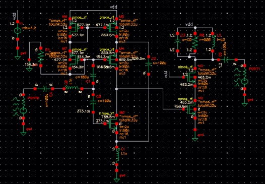
Cadence Circuit Schematic For The Medradio Lna With Integrated Output Download Scientific Diagram

Cadence 8 Noise Analysis Noise Figure Nf Of Lna Using Cadence Virtuoso Tutorial Youtube
Cadence Circuit Schematic For The Medradio Lna With Integrated Output Download Scientific Diagram

Schematic Of The Proposed Lna Download Scientific Diagram

Pdf Design And Analysis Of Low Noise Amplifier Using Cadence Semantic Scholar

Pdf Design And Analysis Of Low Noise Amplifier Using Cadence Semantic Scholar
12 16ghz Lna
Pdf Design And Analysis Of Low Noise Amplifier Using Cadence Semantic Scholar
0 comments
Post a Comment